


5E89 Special-Purpose Computers
Home → Articles → 5E89 Special-Purpose Computers
Yaroslav Khetagurov
Computer engineering in the USSR was progressing in two directions, almost in parallel and independently from each other. The first direction was aimed at creating general-purpose, or universal computers, while the second one - at the development of specialized machines, primarily for military purposes.
Speaking of the latter, extra requirements were placed upon reliability of operation in different conditions and data authenticity. More stringent requirements were also imposed on maintenance in operation. All this strongly affected the design, structure and technology of special computers.
It is obviously important to study the history of development of special-purpose computers, because their development involved ingenious architectures, circuit engineering and design solutions. The emergence of these original solutions was dictated by the very organization of military systems development, where computer hardware had to be based on poorly advanced element base. That was a great impetus for searching non-conventional paths, and sometimes this resulted in the creation of specialized machines and defensive systems exceeding other solutions by many parameters.
The article is devoted to the most interesting special computer models which were produced on a full scale for military systems; some original solutions used in experimental computers are also described here.
Special-Purpose 5E89 Computer
The 5E89 computer ("Kurs-1") became one of the first Soviet mobile specialized machines using alloy transistors and point-contact diodes. The project was under development from 1959 to 1962 at the Naval Research Institute (MNII-1). In 1962 after acceptance trials the computer came to full-scale production. Until 1970 it was manufactured at the Ulyanovsk engineering plant, and later - at the Zagorsk electromechanical works. Production was terminated in 1992. The 5E89 computer was used for secondary processing of real-time data from radars in automated control systems. To increase the system reliability and performance, provision was made for joint operation of two computers.
The computer system was installed on two trailers.
5E89 Computer Specifications
Number representation system - binary with fixed comma after a sign digit. Word length - 20 bits. The numeric part of a word occupies 19 bits and the number sign - 1 bit.
Command system - single-address. Number of bits for instruction codes - 20, including 6 bits for an opcode, 12 bits for an address code, and 2 bits for control tags. Number of operations - 63.
Ferrite-core RAM capacity - 1984 20-bit numbers. Time necessary for access and writing of one number in RAM - 4 clock cycles.
Constant and program memory capacity - 2048 20-bit numbers. This memory is used to store constants and programs which can be changed manually.
ROM capacity - 2048 20-bit numbers. ROM is also used to store constants and programs. The code writing requires installation works - laying of wires through ferrite rings.
While in service two system modernizations were carried. As a result the ROM capacity was increased up to 16,384 numbers at the expense of excepting constant and program memory.
Arithmetic unit - parallel, single.
Computer building-block range - pulse-potential on alloy transistors, point-contact diodes and ferrite-core pulse transformers.
Operating Characteristic of Special 5E89 Computer
The machine is intended for operating at an ambient temperature from 5 to 40°С, air humidity 93-97% at temperature 20-25°С, atmospheric pressure of 460 mm Hg, and can take impact loads up to 8 G.
Power supply - three-phase 220/380 VAC, 50 Hz.
Time for turn-on and preparation of the equipment - 5 min max.
Deployment time during installation - 8 h max. (corresponds to a radar-tracking site deployment time).
5E89 Computer Design
The special-purpose computer consists of:
- arithmetic unit
- control unit
- data exchange unit
- ferrite-core RAM (FCRAM)
- ROM
- management and control console
- three-phase 220/380 VAC, 50 Hz primary power supply of 34,4 kW installed power
- secondary power supply unit
- air-conditioning system including 11.5-kW cooler and 8.4-kW heaters and fans
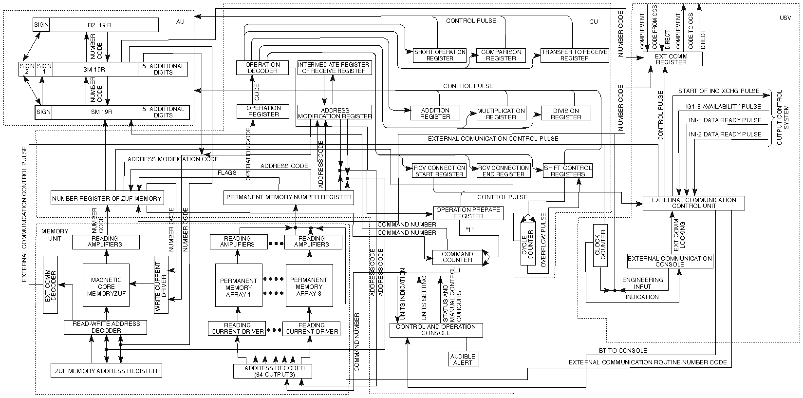
The block diagram of 5E89 computer is shown in Fig 1.
Brief Description of Computer Components
Arithmetic unit (AU). The arithmetic unit is aimed at executing arithmetic and logic instructions both with full and low-bit numbers, and also at address modification and information exchange with external sources.
AU consists of an accumulative type adder and two registers - R1 and R2.
To minimize the multiplication time and to simplify the arithmetic unit logic, the method of multiplying from high bits is used. This method eliminates the necessity of shift in the adder thus increasing the multiplication speed due to overlapping the shift instructions in the registers and additive instructions in the adder.
To get the required instruction accuracy, the capacity of the adder and register R1 is enlarged by five.
Register R2 has 20 bits. The multiplication and division scheme is shown in Fig. 2. The multiplicand is placed into register R1, and the factor - into register R2, the product is calculated in the adder. The number in register R1 is shifted to the right, and in register R2 - to the left.
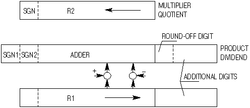
Fig. 2
The dividend is put in the adder, the divisor is written into register R1 and the quotient is formed in register R2. The shifts in the registers correspond to the shifts in multiplication.
The numbers in the adder are represented by the modified one's complements. The adder has two sign bits. The total capacity of the adder is equal to 26 bits (2 sign, 19 main and 5 additional bits). Register R1 has 25 bits (1 sign bit, 19 main and 5 additional bits). Register R2 has 20 bits (1 sign bit and 19 main bits).
Without a word size overflow both sign bits of the adder have an identical value "00" (+) or "11" (-). The values "10" and "01" of sign bits specify a word size overflow (10 corresponds to an underflow, 01 - to a positive overflow).
When a number is sent to AU it always goes to register R1.
Control unit (CU). The control unit carries out the automatic control of the computing process. It performs command and number access from FCRAM and ROM, controls arithmetic and logic instructions execution, and also handles data input/output.
For instruction control signal framing the shift registers are used; they allow combining the stages of instruction execution and minimizing the requirements for the working frequency of devices generating control pulses. In addition, using the registers simplifies adjustment and preventive maintenance, and also makes systems upgrade easier.
The data exchange unit provides link to external resources and supports information exchange with subscribers of the system where the computer works.
The data exchange unit can service up to eight subscribers. Exchange is implemented by sentences containing four or six words of 18 bits each.
Ferrite core RAM. The random access memory on magnetic cores is intended for recording and storing both the raw information and intermediate results. There are three modes of operation: recording, reading and reading with blanking. To minimize the ferrite cube size, the storage cell capacity is 40 bits and two 20-bit numbers are placed in it. Altogether 1984 numbers can be stored in this RAM.
ROM. The read-only memory has a capacity of 16,384 20-bit words and is aimed at the storage of constants and commands. It can operate only in one mode - reading the information. Data entry or change is carried out by reweaving a wire through a matrix. The unit consists of 32 separate removable modules capable of storing up to 512 numbers each. Such a design provides high adaptability to manufacture of ROM and gives a possibility to make quick changes in programs.
Management and control console is intended for computer operation management, testing, program debugging and controlling the machine. The audible signalling of computer program execution is provided.
Primary power supply unit converts a three-phase 220/380 V, 50 Hz current of the industry standard into a two-phase 220 V, 427 Hz current. Conversion is done by motor-generators. To provide high reliability, two such devices are used - main and redundant, with the rated power of 11.9 kW each. The conversion of alternating current from 50 to 427 Hz helps to decrease the size of secondary power supply units and to exclude the influence of network switching interferences on the computing devices operation.
Secondary power supply unit converts the two-phase 220 V, 427 Hz current into the current at a stabilized constant voltage necessary for power supply of different computer units, their protection in emergency modes and for centralized control of secondary power supply units powering on and off. The total power consumed by computer units equals 4.4 kW.
Information Representation in Special-Purpose Computer
The 5E89 computer uses a binary numbering system. The numbers are represented with fixed comma. An absolute value of any number is less than one, the sign of a number is located in the high bit. The numbers are stored in the memory in one's complement. For more effective usage of FCRAM two short-bit numbers can be written in a memory cell and a limited number of instructions can be executed with them.
The following combinations of numbers stored in a cell are possible:
- 13 and 6-bit numbers
- 13-bit and single-bit numbers
- Two 8-bit numbers.
The allocation of numbers in a cell is shown in Fig. 3.
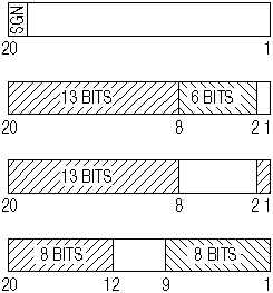
Fig. 3
Numbers with fixed comma can change in the range -1 < - M < -2-19.
System of Instructions
The special 5E89 computer uses a single-address system of instructions. All the instructions here can be divided in two categories: address and zero-address ones. Executing zero-address instructions requires neither extracting numbers from the memory nor writing them into RAM. The structure of instructions is shown in Fig. 4.
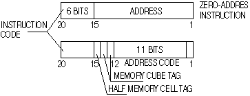
Fig. 4
The address field of a zero-address instruction is used for coding the quantity and direction of shifts in left-and right-shift instructions. The instruction number necessary to execute conditional and unconditional branch instructions is also placed here
This computer supports 63 instructions including 28 arithmetic, 13 transfer, five readdressing register, seven control transfer and three special ones.
To more effectively use the FCRAM and ROM capacity as well as to increase performance, instructions with low-bit numbers were introduced in the special-purpose computer for the first time. The developers estimated that the feature specialized for the particular tasks increased the performance of the machine by 40 to 45 percent compared to the low-bit number packing for reducing its memory capacity.
The following groups of instructions could be executed with low-bit numbers: number writing from the adder to the memory, number transfer to the adder, addition, subtraction, multiplication, and difference modulus calculation. Each instruction in the group gets a specific number depending on the low-bit number position in the memory cells.
Low-bit instructions are executed according to their numbering in the following order.
- Instructions with number 1 are executed with numbers taken from 13 high bits of a memory cell (bits 20-8) and transferred into high bits of arithmetic unit register R1 (bits 20-8).
- Instructions with number 2 are executed with numbers taken from six bits of a memory cell (bits 7-2) and transferred into high bits of arithmetic unit register R1 (bits 13-18).
- Instructions with number 3 are executed with a number taken from the first bit of a memory cell and transferred into the 20th bit of arithmetic unit register R1.
- Instructions with number 4 are executed with numbers taken from eight bits of a memory cell (bits 8-1) and transferred into high bits of arithmetic unit register R1 (bits 19-12).
- Instructions with number 5 are executed with numbers taken from eight high bits of a memory cell (bits 20-13) and transferred into high bits of arithmetic unit register R1 (bits 20-13).
Let us consider the instructions characteristic of the specialized computer. They are "control transfer instructions" and "special instructions". Other instructions are executed according to well-known algorithms, and their description is of no interest.
Control transfer instructions. The instructions of this type are aimed at changing the calculation direction. There are two control transfer instruction types in 5E89. Conditional branch instructions use two algorithms and unconditional branch instructions - five algorithms. Multiple algorithms help to reduce the number of instructions necessary for system problems solving.
Conditional branch No. 1 (CB1) can be address and zero-address. In zero-address instructions an instruction number T is written to its address field. The number belongs to an instruction which takes control when w=0 (the instruction number is put into the instruction counter). When w = 1 control is transferred to the next instruction in the counter.
If the address field of instruction contains a FCRAM tag and "zero" in the 14th bit, the instruction becomes an address one. The instruction number which should take control when w = 0 is extracted by the counter from 14 low bits of the RAM cell with address specified in instruction CB1. When w=1 control is transferred to the next instruction in the counter.
The difference between instructions CB1 and CB2 is that the latter is executed when w = 1, and at w=0 control is transferred to the next instruction.
Unconditional branch No. 1 (UB1) can also be address and zero-address. In zero-address instructions the address field contains the instruction number to which control is transferred (the number is written into the instruction counter). Address instructions have a FCRAM tag and "zero" in the 14th bit. The instruction number which should take control is extracted by the counter from 14 low bits of the RAM cell with address indicated in instruction UB1. Unconditional branch No. 1 instruction is written one instruction earlier than it should be executed according to the program. Instruction UB1 cannot be followed by unconditional branch instructions UB1, UB2, UB3, UB4 and UB5, unconditional branch instructions CB1 and CB2, or instruction IZRP.
Unconditional branches No. 2 (UB2, UB4 and UB5) can be executed by address and zero-address instructions. Zero-address instruction UB2 is executed similarly to zero-address instruction UB1. If the instruction is an address one, it is executed in the same way as UB1, but the instruction address is increased by two in relation to the address indicated in instruction UB2. Unconditional branch instructions UB4 and UB5 fulfil not only switching from ROM111 to ROM 111 (UB4 instruction) but also reverse switching from ROM 111 to ROM111 (UB5 instruction). The emergence of these instructions allow the full use of an adress bit array.
Unconditional branch No. 3 (UB3) can be carried out only by an address instruction, exactly as address instruction UB2.
Special instructions. There are three such instructions: beginning of the communication program (BCP), end of the communication program (ECP) and break.
Instruction BCP is activated by the external communication unit transmitting a signal about availability of any of eight channels. The signal starts the external RAM links decoder which determines the external communication program address. After the next instruction is executed, data from the adder, instruction register RP, instruction counter plus w-tag are written to a certain FCRAM cell. This is necessary for the program to return to the calculations interrupted by exchange. Three memory cells are used when writing the information about the program state. After the instructions are executed the external communication program for a specific subscriber is activated.
Exchange terminates by instruction ECP, which returns all data from FCRAM to previously occupied cells and resumes the program execution. The sequence of subscribers' calls is regulated thus eliminating conflict situations.
The break instruction stops the computer and saves information in main units.
Here is a description of sequence of standard instruction execution on an example of the "addition" instruction. Suppose it is necessary to add the number written in the adder to the number in a memory cell. The cycle is divided in two stages - preparatory and executive. Such a technique increases the computer performance because the preparation for executing one instruction can be fulfilled simultaneously with executing another one. While instruction N is executed, the number for instruction N+1 and instruction N+2 are read off.
Basic Components of Specialized Computer
The special computer hardware is based on P16 transistors and D9 pulse diodes. A pulse-potential technology is used in the computer building-block range. Main memory and counting cells contain a potential flip-flop controlled by starting pulses delivered to the transistor base, and some logics: a pulse-potential diode valve, emitter valves for carry chains and amplifiers of three types. The composition of the computer building-block range was defined after the thorough analysis of various logics for the specialized computer functional devices and available transistors and diodes specifications.
The frequency response and amplification factor of a transistor greatly influenced the choice of component schematic. Special emphasis was placed to the high reliability of the computer building-block range therefore an ingenious flip-flop with controlled complementing input (T-trigger) and custom pulse-potential diode valve (which was much more reliable than transistor valves) were used. To increase the transistor components reliability, the saturated mode was widely used. It ensures a good load characteristic, amplitude stabilization and computer efficacy in the required temperature range, as well as simplifies adjustment and maintenance.
There was a risk of increasing the pulse signal width and lowering the working frequency in saturated modes. To avoid this, pulse transformers and ferrite-core chokes were widely used.
The resulted computer building-block range consisted of a flip-flop with emitter followers, a diode valve, and emitter valves of a carry chain and a ripple-through carry, pulse amplifiers of two types, a powerful emitter shaper, and an indication amplifier.
The effective modes of operation were supported by six main and two auxiliary DC voltages generated at a secondary power supply unit.
The choice of components used in the computer allowed using a minimal range of standard electronic units.
Before the components were installed on cards they were individually checked for compliance with technical specifications to guarantee a high reliability of the computer. The main attention was concentrated on the transistor and diode parameter testing. At the beginning some manufacturers did not check the characteristics of transistors so special test beds were designed to fulfill the task.
To provide a high reliability of hardware, it was tested during manufacturing at test rigs inspecting their serviceability in certain environments.
Let us consider some schematic distinctions of the components used.
The flip-flop is based on a classical scheme with some components added to increase its performance. A cut-off is used to cut the trailing edge of a pulse having the greatest width. To support counting mode, a switched input transformer is used; it increases the switching speed. The load is connected to the flip-flop through an emitter follower to exclude its influence on the speed of operation. To enhance the flip-flop stability in a wide temperature range, an automatic bias is used. There are also two independent inputs to transfer the flip-flop in positions "0" and "1".
The operating frequency of flip-flop is up to 300 kHz. The width of control pulses can be from 1.5 to 2 ms and their amplitude - from 1 to 1.8 V.
The flip-flop can control five - six valves through an emitter follower if they do not operate simultaneously. The schematic diagram of a flip-flop is shown in Fig. 5.
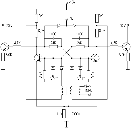
Fig. 5
Valves - coincidence circuits. Potential-pulse valves of two types were developed for a flip-flop.
The first type is a potential-pulse diode valve connected to the emitter outputs of a flip-flop.
The second type is a potential-pulse transistor valve based on emitter followers. It was used for ripple-through and digit-by-digit carry. Such a valve has small pulse latency in a carry chain.
A potential-pulse diode valve, unlike other such devices, has a compensating winding (Fig. 6) which eliminates a known disadvantage of diode-transformer valves - interference at a valve output. This interference depends on the value of output resistance of a signal source and the amplitude of an input pulse. The main advantage of such a circuit is high noise immunity.
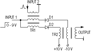
Fig. 6
The input pulse applied to Input 2 can pass to Output (see Fig. 6) only when the voltage at Input 1 equals 9 V. If the voltage at Input 1 is equal to 0, then the pulse sent to Input 2 will not pass to Output. However, if the pulse sent to Input 2 is equal to or greater than 9 V a noise pulse signal emerges at Output. To eliminate it, the pulse from Input 2 in antiphase is applied through diode D2 to the winding of transformer Tr2 thus compensating the noise. The diode valve output is connected to the amplifier input. The picture of a diode valves module is shown in Fig. 7.
Fig. 7
A potential-pulse transistor valve used in chain of carry and chain of ripple-through carry (Fig. 8) has two outputs that differ in values of output signals. Their schematic is based on transistors placed in parallel as emitter followers. The transistor valve operates to close two transistors. To stabilize the emitter potential and to suppress noise, potential diodes D1 and D2 are connected to the base.
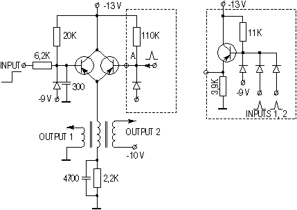
Fig. 8
The only difference between a valve for a ripple-through carry chain and a valve for a carry chain lies in changes in the pulse signal circuit. An emitter follower is installed at the valve input as two input signals are applied. A signal forming function is immanent to transistor valves so they counteract the extension of a signal passing through a carry chain.
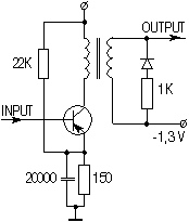
Fig. 9
The operating frequency of valves equals 250 kHz. The signal delay in passing the valve is about 0.1 ms.
Amplifiers. Amplifiers of three types are used in the special-purpose 5E89 computer. All of them work in the saturation mode and are equipped with a stabilizing emitter chain. The register amplifier schematic is shown in Fig. 9. A signal from the diode valve is applied to the amplifier input, its output signal goes to flip-flop control inputs. The amplifier has only one stage. Its operating frequency is up to 300 kHz, the signal delay equals 0.3 ms.
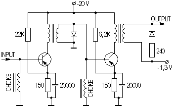
Fig. 10
The schematic of a two-stage amplifier connected to the flip-flop complementing input is shown in Fig. 10. The second stage is necessary because the input resistance of a flip-flop complementing input is lower than that of a control input. The forming function of an amplifier is achieved by the use of chokes which accelerate the clean-out of minor carriers thus increasing the operating frequency of an amplifier up to 300 kHz. The signal delay in passing the valve is 0.5 ms. The picture of an amplifier module is shown in Fig. 11.
Fig. 11
An amplifier-shaper with emitter output (Fig. 12) is used for pulse regeneration and their power amplification. The shaper can service from 20 to 30 amplifiers and from 7 to 8 diode valves. The operating frequency of the amplifier-shaper equals 250 kHz, the signal delay is about 0.5 ms.
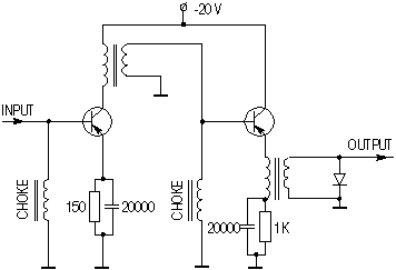
Fig. 12
An indication amplifier is used to demonstrate a flip-flop state (Fig. 13). The main task is matching a neon tube firing potential with the permissible operating voltage of a transistor equal to 20 V.
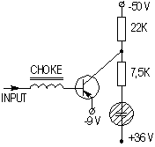
Fig. 13
Design of Specialized 5E89 Computer
The equipment of the special computer is placed in two trailers. One of them contains the computer and auxiliary devices, the other - motor generator based converters, a capacitor, spare parts and different tools.
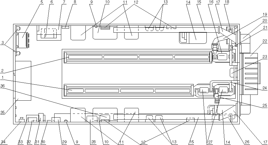
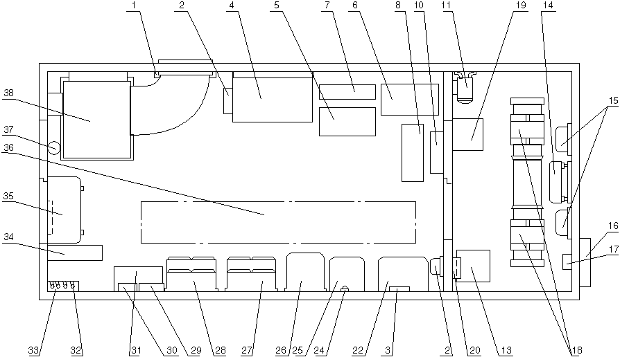
A lay-out diagram of the equipment in the first trailer is shown in Fig. 14. Figure 15 demonstrates the equipment location in the second one. The latter has two compartments - a main bay (I) and a power room (II).
Devices 1 and 2
Devices 1 and 2 form a special-purpose computer. They are installed on a metal sheet and covered with a metal cover (inside cables connect the devices).
The device construction is welded from rolled stock and divided into two sections with board compartments. Each compartment accommodates two circuit boards placed one above the other. They are closed from two sides by plane quick-detachable covers. The circuit board has 60 slots (arranged in six horizontal rows with 10 slots each) used for the installation of modules with electronic components. The slots are equipped with 32-pin connectors. The guiding racks installed on circuit boards provide easy mating of modules and connectors. The modules are inserted from the face part of a circuit board. The mounting side of the board contains terminal blocks and combs with holes for cable assembly installation. Connecting the circuit boards located both in devices or between them is made through connectors located on board edges.
At the bottom of the board a panel with eight fuses and a power plug is installed. The power to circuit boards is supplied through copper buses passing through all compartments. The power supply buses are stacked; each of them has soldering tags for cable assembly wires.
Standard Module
The frame of all modules is made of two identical aluminum alloy argon-arc welded calipers. The shape of the module frame guarantees its rigidity, and side grooves function as guides during installing the block into the board slot. There are eight dimensional stops protecting discrete components. A handle is fastened to the frame front panel, where the serial number and type of the module and an arrow indicating its correct position are given. On the opposite part of the frame a 32-pin plug is installed. The frame also accommodates two standard printed circuit boards made of paper-based laminate 1.5 mm thick. They are manufactured by a method of photochemistry with discrete components. The boards are connected to the plug with a cable.
To provide the reliability of a contact in a 32-pin connector, a new method was found. A special connector structure was designed, which produced a good contact between a plug and a socket during computer tuning-up, and then this contact was soldered thus eliminating the contact deterioration due to mechanical and climatic effects. The after-soldered connectors used for the first time in 5E89 machine guaranteed high operating characteristics and eliminated the contact faults without gold plating. To change such a module, it was necessary to de-solder and then solder again the contacts. Sure this made the process of malfunctions correction a little bit longer but thanks to high reliability did not influence the computer maintenance greatly. The module and the connector are shown in Fig. 16.
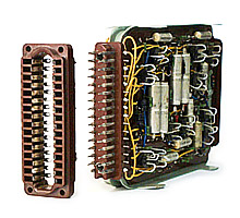
Fig. 16
Legend for figure 14
1 - Device 2 with power supply units 2/1 and 2/2
2 - Device 1 with power supply units 1/1
5 - Device 108 (power distributor to devices)
6 - Trailer lighting transformer
7 - Shelf for gas-masks
8 - Clock
9 - Thermometer
10 - Folding table
11 - Folding chair
12 - Electrical distribution box
13 - Electrical heater
15, 17 - Forced ventilation air duct
16 - Cover of power supply unit 1/1
18 - Device with ballast resistors
19 - Air duct for cooling of power supply unit 1/1 and device 18
20 - Air delivery duct
21 - Left air duct for power supply unit 1/1 and device 18
22 - Frame covered with encasement where in electric motors with centrifugal fans are installed
23 - Service table
24 - Right air duct for power supply units 2/1 and 2/2
25 - Air duct for cooling of power supply units 2/1 and 2/2;
26 - Box with spare parts
27 - Cover of power supply units 2/1 and 2/2
28 - Distribution box
29 - Telephone with loudspeaker
30 - Cable box-coupling
31 - Subscriber box
32 - Camp telephone
33 - Loudspeaker
34 - Howler
35 - Entrance blinds
Legend for figure 15
1 - Box-coupling for communications between trailers
2 - Two electrical heaters
4 - Cabinet for services staff
5 - Box with air-conditioner spare parts
6 - Box with specialized computer spare parts
7 - Box with spare parts for power supply generators AL4
8 - Box with oscilloscope
10 - Box with spare parts for trailer chassis
11 - Two transformers for trailer lighting and air-conditioner power supply
12 - Spare parts box
14 - Device 108 used to switch over power supply units
15 - Starter for main and back-up power supply units
16 - Box with entrenching tools in encasement
17 - Power supply units blower
18 - ALA-type converter (rotary generator)
19 - Step-down transformer
20 - Distribution box
22 - Folding table
24 - Thermometer
25 - Folding chair
26-28 - Cabinets with spare parts for specialized computer
29 - Camp telephone for communications between trailers
30 - First-aid kit
31 - Racks for weapons and gas-masks
32 - Grounding posts
33 - Post mounting
34 - Box for grounding posts cabling
35 - Entrance blind
36 - Bags with inter-trailer communications in field
37 - Spare freon vessel
38 - Air-conditioner